Process node
The name of a generation of chip manufacturing, like "3 nm". A label, not a size.
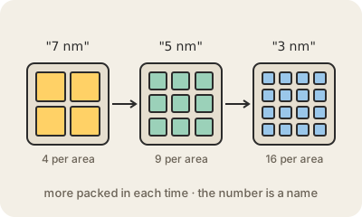
A process node is the name a chipmaker gives to one generation of its manufacturing technology: "7 nm", "5 nm", "3 nm" and so on. Each new node packs transistors more tightly, so a chip of the same size can hold more of them, run faster or use less power, usually some mix of the three. Companies like TSMC, Samsung and Intel compete hard to reach the next node first, and phone and computer makers advertise which node their chips are built on.
Here is the catch: the number no longer measures anything on the chip. Decades ago it roughly matched the length of a part of the transistor called the gate. From the late 1990s on, names and physical sizes drifted apart, and today a "3 nm" chip has no feature that is 3 nanometers long; its key dimensions are several times larger. Transistors did keep shrinking and improving, largely by changing shape and going three-dimensional, but the names simply kept the old rhythm, each one roughly 0.7 times the previous.
So read the node as a brand for a generation: useful for comparing one company's chips over time, much less so across companies. Intel's former "10 nm" was roughly as dense as TSMC's "7 nm", which is one reason Intel renamed its later nodes. For a real comparison, engineers look at transistor density (how many transistors fit in a square millimeter) and at measured speed and power. The node names are a shorthand for the story of Moore's law, not a ruler.
Keep in mind
- A node is a generation of chip manufacturing, named like "5 nm" or "3 nm".
- Each new node fits more transistors in the same space, for more speed or less power.
- The number is a label: no part of a "3 nm" chip is 3 nm long.
- Compare chips by transistor density and measured results, not by node names.
Go deeper
- 3 nm process on Wikipedia
- Semiconductor device fabrication on Wikipedia
- A better way to measure progress in semiconductors (IEEE Spectrum)